REQUEST A QUOTE / ENQUIRY FORM
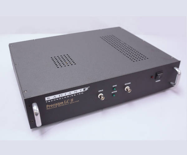
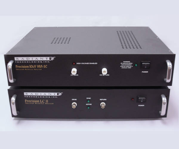
Precision LC II Ferroelectric Tester
The Precision LCII is Radiant's answer to a growing need for affordable characterization equipment. The Precision LCII is an ideal general-purpose tester with a broad test range for thin films and bulk ceramics. The Precision LCII tester has a frequency rating of 5KHz at +/-200V built-in to the system. Using up to 32,000 points with18-bit resolution from 2kHz out to 1/30th of a Hertz for capacitors ranging from square microns to square centimeters, the LC II enables high resolution characterization for bulk capacitors. The Precision LCII II is offered with a variety of internal amplifiers. The Precision LCII is offered in a ±10V, 30V, 100V, 200V, and 500V built-in drive volt option. The Precision LCII can be expanded to 10kV with the addition of a high voltage interface and amplifier.
| Tester Parameter | LC II |
| Voltage Range (built-in drive voltage) | ±10V, ±30V, ±100V, ±200V or ±500V built-in |
| Voltage Range with an external amplifier and high voltage interface (HVI) | 10KV |
| Number of ADC Bits | 18 |
| Minimum Charge Resolution | <10fC< /td> |
| Minimum Area Resolution (assuming 1 ADC bit = 1μC/cm2) | <1μ2< /td> |
| Maximum Charge Resolution | 276μC |
| Maximum Area Resolution (assuming saturation polarization = 100μC/cm2) | 2.76cm2 |
| Maximum Charge Resolution with High Voltage Interface (HVI) | 27.6mC |
| Maximum Area Resolution (assuming saturation polarization = 100μC/cm2) w/o HVI | >100cm2 |
| Maximum Hysteresis Frequency | 5KHz @ 10V 5KHz @ 30V 5KHz @ 100V 5KHz @ 200V 2KHz @ 500V |
| Minimum Hysteresis Frequency | 0.03Hz |
| Minimum Pulse Width | 50μs |
| Minimum Pulse Rise Time (5V) | 40μs |
| Maximum Pulse Width | 1s |
| Maximum Delay between Pulses | 40ks |
| Internal Clock | 25ns |
| Minimum Leakage Current (assuming max current integration period = 1 seconds) | 1pA |
| Maximum Small Signal Cap Frequency | 20KHz |
| Minimum Small Signal Cap Frequency | 1Hz |
| Output Rise Time Control | 103 scaling |
| Input Capacitance | -6fF |
| Electrometer Input All Test Frequencies for all test at any speed | Yes |
| * The minimum area resolution under actual test conditions depends upon the internal noise environment of the tester, the external noise environment, and the test jig parasitic capacitance. | |
| *** Tester specifications are subject to change without notice. | |